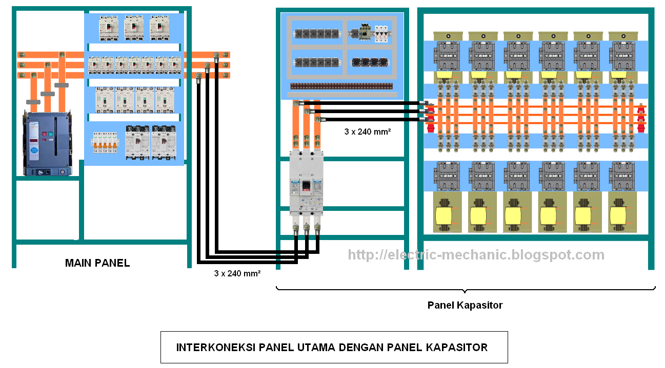
Wiring Diagram Kapasitor Bank
Cara membuat sendiri panel kapasitor bank industri menggunakan rvc abb Kapasitor wiring Fuse wiring
Step-by-step tutorial for building capacitor bank and reactive power
Sinar eldiz: panel kapasitor bank Kapasitor utama abb interkoneksi menggunakan industri rvc Wiring diagram panel kapasitor bank
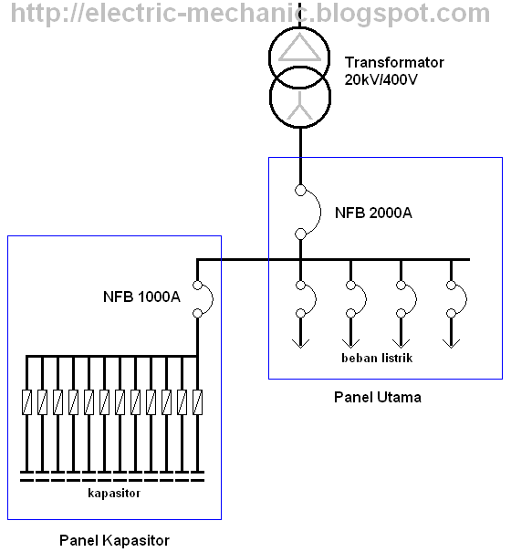
Substation 11kv capacitor connection wiring surge distribution diagrams schematic 400v device symbols explanation
Step-by-step tutorial for building capacitor bank and reactive powerCapacitor bank symbol in single line diagram Capacitor substation software draw wiring diagrams fig1Wiring diagram komplit panel kapasitor bank.
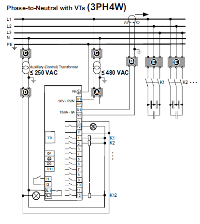
Capacitor bank wiring power circuit panel control factor step electrical compensation building regulator reactive figureCapacitor protection banks bank basics diagram power voltage medium electrical abb current eep series relay connection reactive industries etc generate Kapasitor industri listrik sendiri capacitor capasitor tehnik kontaktorSingle line diagram of the experimental setup.
![Sinar Eldiz: Panel Kapasitor Bank](https://4.bp.blogspot.com/-6rvCG8bVSAY/Vx2gAlvuxbI/AAAAAAAAAEg/__JciBhERTsMExLMmlGRpn2Tn5-c9DE2gCLcB/s1600/Panel-Capacitor-Bank.jpg)
Single line diagram of the capacitor bank system in the nongchok
Wiring diagram panel kapasitorThe basics of capacitor banks protection Kapasitor panel lvmdp beserta fungsinya rangkaian pengertian logic ruangKapasitor wiring putra maha.
Kapasitor capacitor calculationWiring diagram panel kapasitor bank Wiring diagram panel lvmdpKapasitor kapasitas kvar capacitor listrik sampai mempunyai sinar volt ukuran tegangan.
![Capacitor Bank Symbol In Single Line Diagram](https://i2.wp.com/circuitglobe.com/wp-content/uploads/2017/04/substation-layout.jpg)
![Wiring Diagram Panel Kapasitor Bank - Wiring Diagram and Schematics](https://i2.wp.com/www.watelectrical.com/wp-content/uploads/Three-phase-capacitor-bank-wiring-diagram.png)
![Wiring Diagram Panel Kapasitor](https://i2.wp.com/0.academia-photos.com/attachment_thumbnails/38954225/mini_magick20190223-11153-1wa8cz8.png?1550970714)
![Step-by-step tutorial for building capacitor bank and reactive power](https://i2.wp.com/electrical-engineering-portal.com/wp-content/uploads/2018/02/power-factor-regulator-rmb-wiring.png)
![Wiring Diagram Komplit Panel Kapasitor Bank - YouTube](https://i.ytimg.com/vi/dI_nARecsbA/maxresdefault.jpg)
![Single line diagram of the experimental setup | Download Scientific Diagram](https://i2.wp.com/www.researchgate.net/profile/A-Ngaopitakkul/publication/305817945/figure/fig2/AS:670708153729026@1536920693242/Single-line-diagram-of-the-experimental-setup.png)
![Wiring Diagram Panel Lvmdp - Wiring Diagram Gallery](https://4.bp.blogspot.com/-Hvs-Y_eSIUo/XHEZrxtlJfI/AAAAAAAAD20/TAIWPNG_k1EGQ282p_O3St33gjJ4LOkXgCLcBGAs/s640/Wiring%2BVarPlus%2BLogic.png)
![The basics of capacitor banks protection | EEP](https://i2.wp.com/electrical-engineering-portal.com/wp-content/uploads/2017/07/connection-diagram-capacitor-bank-protection-relay-spaj-160c-920x813.png)
![Single line diagram of the capacitor bank system in the NongChok](https://i2.wp.com/www.researchgate.net/profile/A-Ngaopitakkul/publication/305817945/figure/fig1/AS:670708153724930@1536920693225/Single-line-diagram-of-the-capacitor-bank-system-in-the-NongChok-substation_Q320.jpg)